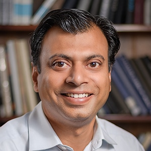
Sumit Agarwal
Professor, Chemical and Biological Engineering
 My research interests are focused on the synthesis and characterization of solar and electronic materials. A significant part of our focus is on plasma-assisted materials processing to achieve atomic scale control over growth and removal of materials to enable the fabrication of next-generation devices. Future electronic devices or solar cells will consist of few-atom-thick sequential layers of metals, dielectrics, and semiconductors that can be as thin as 1.5–2.0 nm. In addition, in semiconductor devices, these layers will be grown or removed selectively using atomic layer deposition or etching to fabricate nanoscale device structures. Achieving this degree of atomic scale control in materials processing necessitates novel surface chemistries and techniques for measuring the chemical composition, microstructure, and the electrical and transport properties. Our research takes a fundamental approach where we use advanced characterization tools to understand interfacial phenomena, and surface and bulk defects in solar and electronic materials. Our group actively collaborates with the semiconductor industry and the National Renewable Energy Laboratory (NREL).
Contact
443 Alderson Hall
1613 Illinois Street
Golden, CO 80401
(303) 273-3508
sagarwal@mines.edu
(Joint appointment with NREL)
Research Group
- Kejun Chen, Drexel University
- Carolina Lima Salles, Montana State University
- Chirag Mule, Institute of Chemical Technology, Mumbai
- Dirk Steyn, University of Florida
- Xue Wang, Purdue University
- Andrew Kaye
- Wallis Scholl
Education
- B.Tech. – Indian Institute of Technology, BHU, Varanasi, India
- M.S. – University of New Mexico
- Ph.D. – University of California – Santa Barbara
- Post-Doctoral Study – University of Massachusetts – Amherst
Selected Publications
- “Understanding the charge transport mechanism through ultrathin SiOx layers in passivated contacts for high-efficiency solar cells, A.S. Kale, W. Nemeth, H. Guthrey, E. Kennedy, A.G. Norman, M. Page, M. Al-Jassim, D.L. Young, S. Agarwal, and P. Stradins, Phys. Lett. 114, 083902 (2019).
- “Atomic layer deposition of silicon-based dielectrics for semiconductor manufacturing: Current status and future outlook,” R.A. Ovanesyan, E.A. Filatova, S.D. Elliott, D.M. Hausmann, D.C. Smith, and S. Agarwal, J. Vac. Sci. Technol. A 37, 060904 (2020).
- “Etch selectivity during plasma-assisted etching of SiO2 and SiNx: Transitioning from reactive ion etching to atomic layer etching,” R.J. Gasvoda, Z. Zhang, S. Wang, E.A. Hudson, and S. Agarwal, J. Vac. Sci. Technol. A 38, 050803 (2020).
- “Influence of tabula rasa on process- and light-induced degradation of solar cells fabricated from Czochralski silicon,” A. R. Meyer, V. LaSalvia, W. Nemeth, W. Xu, M. Page, D. L. Young, S. Agarwal, and P. Stradins, IEEE J. Photovolt. 10, 1557 (2020).
- “Isolating p– and n-doped fingers with intrinsic poly-Si in passivated interdigitated back contact silicon solar cells,” M.B. Hartenstein, W. Nemeth, V. LaSalvia, S. Harvey, H. Guthrey, S. Theingi, M. Page, D.L. Young, P. Stradins, and S. Agarwal, IEEE J. Photovolt. 10, 1574 (2020).
Honors & Awards
- 2009 NSF CAREER Award
- Fellow of the AVS